| |
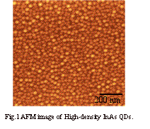
Self-assembled semiconductor quantum dots (QDs) are much attractive for various device applications: QD laser, single photon source and detector, quantum computing, single electron transistor and memory, spin-controlled devices and so on. In order to realize such QD devices, the QD structure must be controlled precisely. In particular, a large inhomogeneous broadening in the QD structure is one of important problems. In addition, high QD density is also requested for realization of QD lasers with high performance. Recently we have demonstrated high-uniformity and high-density InAs QDs on GaAs(001) substrates by Sb-mediated Stranski-Krastanov (SK) growth method. The underlying Sb-terminated GaAs layers enhanced the nucleation of the three-dimensional (3D) InAs islands, and high QD density of 1×1011 cm-2 was achieved successfully, as shown in Fig.1. |
|