Monitoring and Control of Epitaxial Growth by Optical Reflectance
Professor Naoki Kobayashi
naoki@pc.uec.ac.jp
http://www.pc.uec.ac.jp/
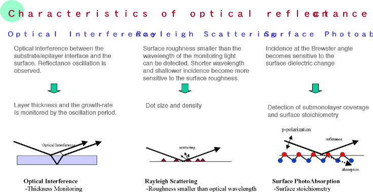
Electronic and optical devices using compound semiconductors such as GaAs and GaN consist of thin-layered structures fabricated by the epitaxial growth. Practical devices of two-dimensional electron gas FETs and quantum-well lasers are grown by Metal Organic Vapor Phase Epitaxy ( MOVPE ) having an ability of precise control of the layer thickness and the composition of the layer material. Recent progress in quantum devices requires a strict control of the growth. For example, in the growth of quantum dots (QDs), the control of not only their size in nm-scale but also of their density are indispensably required to avoid a subband-level fluctuation and to control the quantum correlation between dots. For this purpose, in-situ observation of the surface during growth enables to measure the dot size and density.
Optical reflectance is an effective method of monitoring the surface in the vapor phase epitaxy, instead of the electron probe used in the vacuum. Up to now, we succeeded in the monitoring of the decomposition process of organometallic molecules on the surface and the chemical stoichiometry of the surface during growth. Recently we try to clarify the surface process in GaN MOVPE, which is a large lattice-mismatched growth, and to characterize the surface roughness related to the dot size and density in real time by using the optical reflectance monitoring.